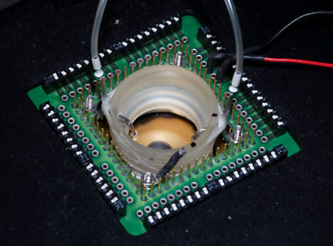
At SPLITZDESIGN, we have years of experience in designing a wide range of printed circuit boards from a simple single layer thru-hole to complex multi-layer, double sided surface mount designs that meet or exceed all of our customer’s electrical and mechanical constraints.
Our PCB Design team of in-house electrical engineers can handle your toughest designs. In time critical design our team works around the clock. Our PCB Expertise Center has capability, experience and expertise to effectively support our customers in their most complex PCB designs and pressing deadlines.
Whether we lay your board out at our facility or yours, you can expect the same premier service that has created our growing number of loyal design customers. Processes and tools used to design printed circuit boards vary from company to company. Variations of design flows are too numerous to list but typically involve all or some of the following
Design and architecture specification
- HW architecture description
- Cost analysis
- Interface and bandwidth definitions
- SW programming sequences
- EMI design practices
Design Entry
- Graphical design entry from company libraries
- Symbol and part number generation if necessary
- Simulatable vhdl or verilog netlist generation
- Build netlist generation
- BOM generation
- Parts list generation
Purchasing and Vendors
- Preferred vendor lists
- Cost negotiations
- Part obsolescent avoidance
Mechanical
- Board shape, connector placement, etc
- System level faraday enclosures
Manufacturing
- Design for test issues (bed of nails, jtag, etc)
- Interaction with layout house (or on site), oversee layout
- Interaction with board assembly house
PCB Design Tools
- Mentor Graphics™ Expedition™
- Mentor Graphics™ PADS Layout™
- Cadence-Allegro™
- Protel™
Standard Layout Documentation Package
- Fabrication & Assembly drawings
- Gerber, NC Drill, ICT, BOM and X-Y pick-n-place files
- Database files
Standard Layout Documentation Package
- Debug with the SW team
- EMI testing
- Thermal testing
- High reliability mixed digital and analog subsystem design
- Design for fault isolation and diagnostic visibility
- Design using worst case and failure modes and effects analysis
- Layout specifications for EMC and reduced EMI
- Circuit Board Design and Layout
- Built for test ASIC/FPGA evaluation circuit board design
- Reference design and breadboard circuit boards
- Layout specifications for EMC and reduced EMI
|
